Adisyn (ASX: AI1) has a second US patent allowance in the bag, and this one might be even better than the first.
The first, allowed in May, was built around the way AI1 makes its graphene. This one protects the graphene-coated products themselves, whoever makes them and however they get there.
And a US allowance is the one you want. The chip industry’s biggest players live there, and so do the courts where patent fights are worth winning.
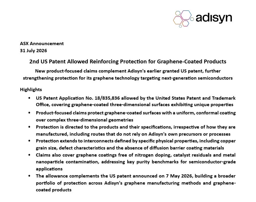
The claims in this second patent are written around the end product and its specifications, which means the protection holds even if a competitor arrives at the same result using a completely different process.
So say someone like Samsung spends the next five years and a few hundred million dollars working out its own way to coat chip wiring in graphene. Their own chemistry, their own machines, none of AI1's process anywhere near it.
If what comes out the other end matches the specs in AI1's claims, Samsung is still writing AI1 a cheque.
The lawyers’ version reads “irrespective of how the coated surface or interconnect is produced”, which is a dry way of saying there’s no back road around it.
Where AI1 Sits
A quick recap for anyone joining late.
AI1 spent six years working out how to grow graphene, a sheet of carbon one atom thick, inside the machines already running in the world's chip factories.
We added AI1 to the portfolio in April at 6.8 cents. It trades at 12.5 cents today, and it’s been a rare week since April that the company hasn’t given us something to write about.
April was the coupon: a full 1cm by 1cm square (about the size of your thumbnail) covered in continuous graphene, grown inside one of those machines (an industrial ALD unit) at a temperature a chip factory can survive.
Nobody had managed that before.
May was the first US patent allowance and the exclusive stealth drone licence with Tel Aviv University. Along the way came a $14 million placement cornerstoned by Meitav and Regal, and retired Colonel Tamir Zimber, the operational commander of Iron Dome, joining the drone subsidiary’s advisory board.
The drone work and the chip work run off the same graphene platform. One side of it coats an aircraft so radar sees less of it. This patent belongs to the other side, the wiring inside advanced chips.
Chips are the processors inside everything from your phone to your computer to your car to every AI data centre in the world, and the industry that makes them is on track for close to a trillion US dollars this year.
Every advanced chip on the planet has the same wiring problem. Copper has been shrunk so thin that resistance is climbing, and AI workloads now waste staggering amounts of electricity just pushing electrons through it, which is a strange problem to have created for ourselves, but here we are.
The chip industry settled on graphene as the fix over a decade ago, but nobody could make it at temperatures that don’t melt the chip.
AI1 cleared that hurdle on the coupon, and the job now is proving the result repeats across hundreds of samples under factory conditions.
What the New Patent Covers
The May patent covered AI1’s method and what it produces. The new one attaches to the products themselves: graphene coatings that hold an even layer over complex three-dimensional shapes, and interconnects, the microscopic copper wires that carry signals around a chip.
Everything AI1 is doing on the semiconductor side ends at the interconnect.
The protection itself lives in the claims, the list of specifications every patent is built around. If you build something that matches the list then you’re infringing on the patent.
Claims are understandably written in patent-speak, so here they are straight from the announcement, with our translation underneath:
a median copper grain size under 0.9 microns
fewer shorts and voids than a comparable interconnect exposed to 400°C or more
interconnect metal substantially free of diffusion barrier coating materials
graphene free of nitrogen doping, FeCl3 residuals and residual metal catalyst nanoparticles
Grain size is how the copper crystals form inside the wire, and it decides how well the wire moves electricity and handles heat.
Shorts and voids are the tiny manufacturing flaws that kill chips, and chip production runs hot enough to cause plenty of them. This claim is for wiring that comes through the heat with fewer flaws than standard copper manages.
Copper also has a bad habit of bleeding into whatever sits around it, so every copper wire in a chip gets wrapped in a protective layer to hold it in. That wrapping steals precious room inside wiring that’s already impossibly thin. Wiring that skips the wrapping altogether is covered too.
The last one is purity. Contamination has crippled rival graphene processes for years, because graphene carrying leftover chemicals or stray metal particles is useless inside a chip. The final claim covers the clean version, which is the one the industry has been waiting on.
Managing director Arye Kohavi:
“These characteristics are directly relevant to the challenges facing next-generation semiconductors. Copper grain size and reduced shorts and voids can influence electrical resistivity and thermal performance, while removing conventional diffusion barrier materials may create additional space as processors continue to scale.”
The patents are now the part of AI1’s moat you can read. But the precursor chemistry and years of accumulated know-how stay locked up as trade secrets, unpublished and never expiring.
The Bigger Prize
AI1 could one day license this technology to several chipmakers at once, and a patent over the product itself gives the company far more to charge for than a patent over one manufacturing route ever would.
A prospective partner wants enforceable US protection over the method and the finished article before signing anything. As of this week, AI1 has both.
The Selloff and the Spending
More than a trillion US dollars has come off chip stocks this month (Intel alone is down more than 20%) as Wall Street asks whether record AI spending can hold its pace.
Alphabet used its latest result to lift its 2026 capex forecast in spite of it. Chip giant TSMC, which manufactures for just about everyone, beat profit and revenue expectations in July while flagging even more capital spending than planned.

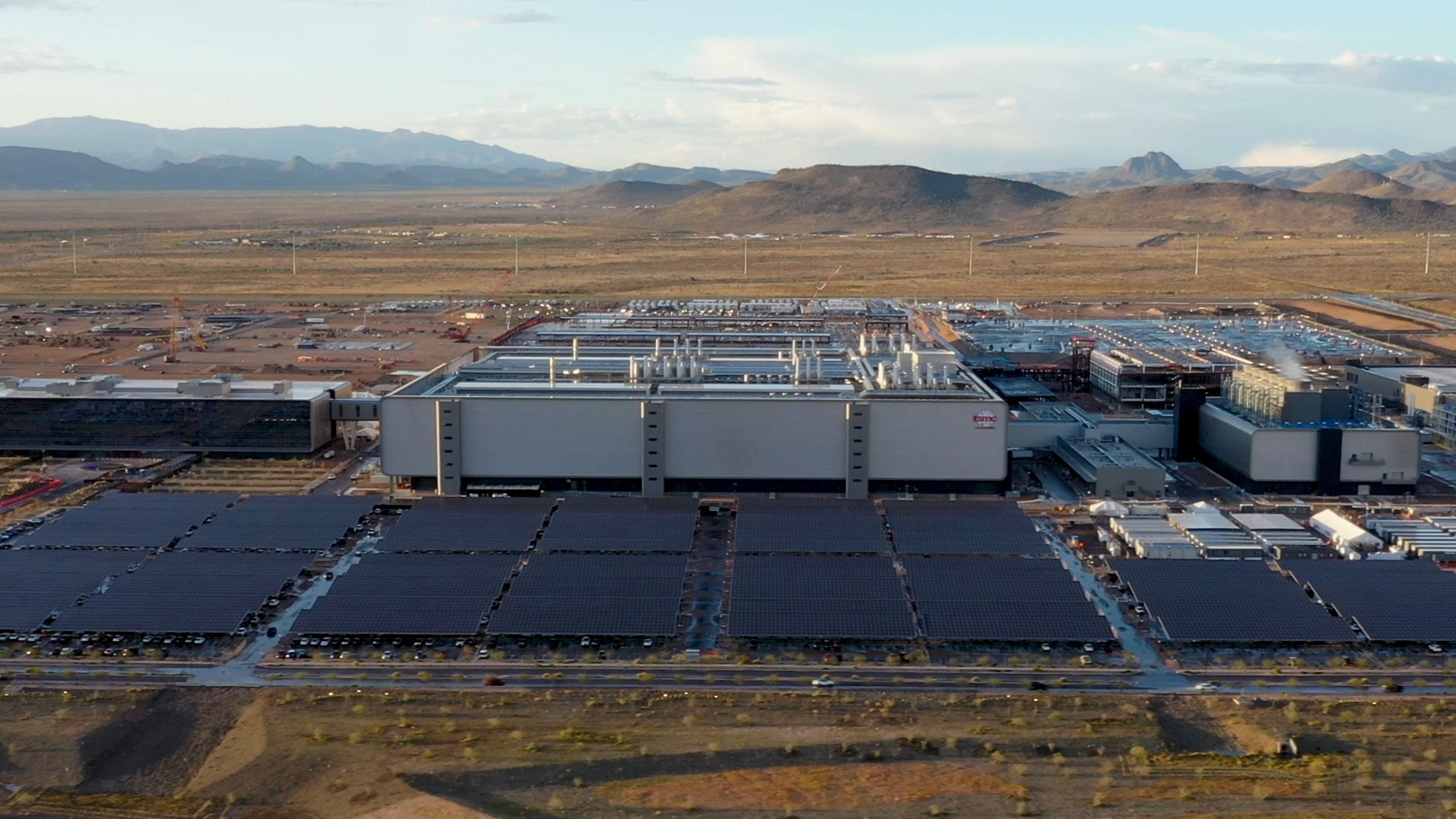
Then there's the CHIPS Act money behind TSMC's Arizona fabs, the giant factories where chips get made, and the billions Micron and Samsung are putting into plants still under construction.
The government pays it out in tranches as construction milestones get ticked off, so much of it hasn't even landed yet. Every fab it builds will need next-generation materials from the day the doors open.
Each one of those fabs inherits the same copper problem AI1 is working on, selloff or no selloff.
What We’re Watching
Both patents still need their formal grant, and with the examiner's call already made, the official stamps usually land within a few months.
AI1 has flagged patent applications in other jurisdictions too, so expect the wall to keep rising beyond the US.
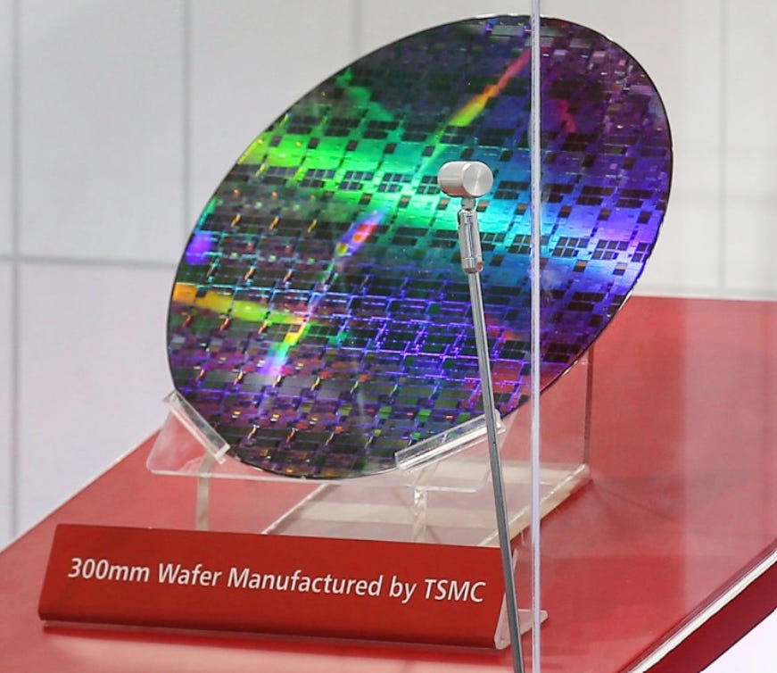
AI1 has covered a 1cm by 1cm coupon in continuous graphene, and a commercial fab builds on 300mm wafers. Getting from one to the other is the difference between a lab result and a product a factory can run, and it’s the milestone we’re watching closest.
AI1 is talking to potential partners and customers across both the chip and radar programs, and two granted-track US patents give those conversations a firmer footing than lab results on their own ever could.
A patent protects the technology without making anyone adopt it, and the wafer scale-up over the next 12 months is where AI1 starts making its case.
If the industry makes the jump, whoever moves first, the door they knock on belongs to AI1.