

Adisyn Just Cracked Graphene's 300°C Wall
The breakthrough the whole chip industry has been chasing for a decade, signed off by an independent expert.

The chip industry has spent decades trying to grow graphene inside a finished chip without cooking everything around it.
Adisyn (ASX: AI1) just cracked the code.
It deposited the graphene below 300°C, and it did it run after run. No previous graphene process has worked below the industry's thermal limit, anywhere.
Copper is the wiring buried inside every advanced AI chip on the planet, and it’s hit its physical limits. TSMC, the biggest chipmaker on earth, has already named graphene as the way past it, and Adisyn is the first to deposit graphene at a temperature a chip can survive.
This is a trillion-dollar-a-year industry, and an ASX small-cap just delivered the result that makes Samsung, TSMC and Intel sit up and pay attention.
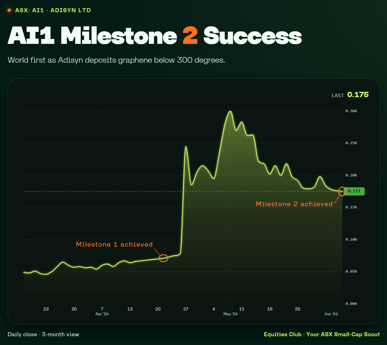
Adisyn is one of our portfolio holdings. We first wrote it up for readers in April at 6.8c, and it's up more than 150% since then, with the biggest catalysts still in front of it.
Today’s result clears the way for the big one, a commercial deal with one of the global chipmakers, and that’s what management is chasing inside the next 12 months.
AI1 made the breakthrough, then did the thing most small-caps avoid. It handed the raw data to someone independent and let them pull it apart.
That someone trained alongside the man who won the Nobel Prize for discovering graphene.
His name is Associate Professor Rakesh Joshi, who runs the Graphene Research Group at UNSW. He went through Adisyn’s data, across repeat runs and multiple points on the sample, and confirmed it stacks up.
The Man Who Checked the Work
In 2010, two scientists at the University of Manchester won the Nobel Prize in Physics for a material they had peeled off a block of graphite using ordinary sticky tape.
The material was graphene. A single sheet of carbon atoms, stronger than steel and a better conductor than copper, and their work turned it from theory into something you could hold.
One of those two scientists was Sir Andre Geim. Early in his career, Rakesh Joshi worked under Geim at Manchester and co-authored research with him.
These days Joshi is an associate professor at UNSW, where he leads the university’s Graphene Research Group and has published more than 130 papers in the field. Few people on earth are better placed to look at a set of graphene results and tell you whether they hold up.
So Adisyn handed him everything. The same deposition process run three times on three separate days, plus dozens of measurements taken at points right across each sample.

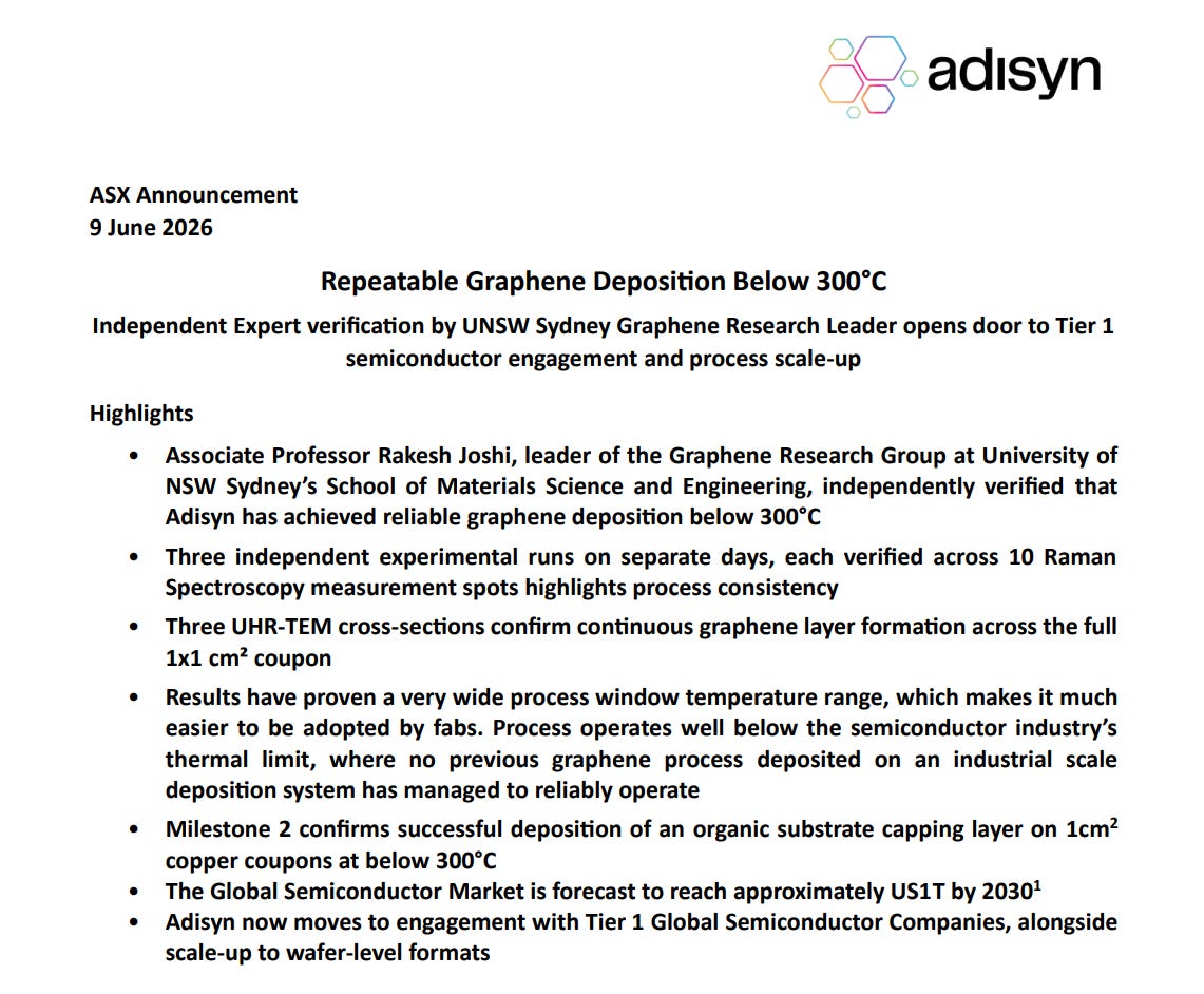
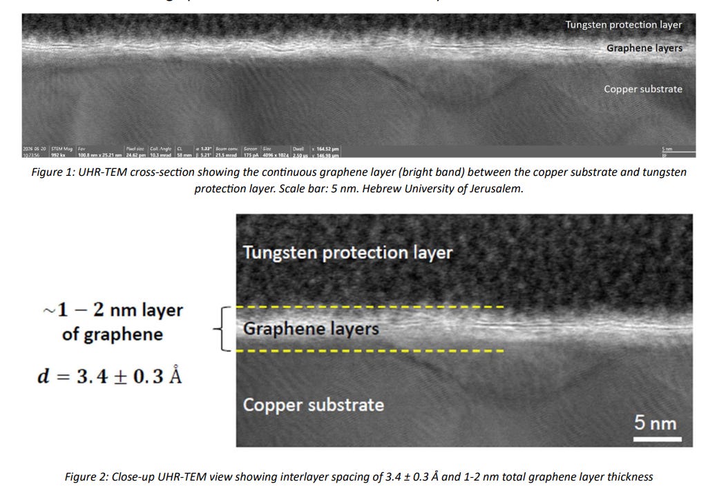
Each of those samples is a small square of copper, about a centimetre a side, with the graphene grown on it. By grown we mean carbon is laid down inside a chamber and the atoms settle into a single layer, one atom thick, across the copper.
One set of tests shows the result repeats, the other shows it’s even across the whole surface.
Joshi, who doesn’t work for Adisyn and has no stake in the outcome, went through the lot and confirmed the graphene is real, and that the process does what Adisyn says it does.
Plenty of companies say their science works. Not many are confident enough in the results to hand an outsider of that calibre the raw data and invite him to prove it doesn’t.
Why the Temperature is the Whole Game
Every advanced chip today runs on copper. Billions of transistors, all linked by copper wiring far too fine to see, moving electricity around the chip.
Copper has worked beautifully for decades. The problem is what's happening now the wires have shrunk this far.
The newest chips are shrinking below two nanometres, and at that scale copper starts to choke. Resistance climbs and the wiring runs hot, so power that should be doing useful work leaks away as heat. Across a data centre full of AI chips, that waste turns into a power bill big enough to run a small city.
The industry has known the fix for years. Graphene moves electricity more efficiently than copper, and it keeps doing it at sizes where copper overheats and fails.
Graphene was always going to work. The hard part was making it.
Growing it the usual way takes heat of around 1,000°C. A chip is a delicate stack of materials, and anything past about 450°C starts to wreck the structures already built into it. So the one material that could save the chip had to be grown at a temperature that would destroy it.
That’s the wall. Every chipmaker on earth has been staring at it for a decade.
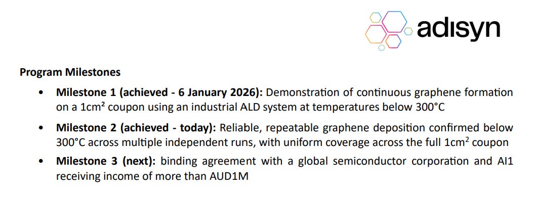
Adisyn just grew graphene below 300°C. Comfortably under the ceiling.
Anyone Can Get Lucky Once
The customers Adisyn is chasing are the giant chip factories, known in the industry as fabs.
TSMC, Samsung and Intel run them, and none of them will build a billion-dollar production line around a coating that worked one Tuesday and never again. So this result was about proving the first one would repeat.
Adisyn ran the same process three times, on three separate days. Same recipe, same setup, and each run produced the same graphene layer.
Then they checked the layer was good across the whole square, not just in one spot. When you grow a coating this thin, the danger is it comes out patchy, solid in one part and thin or missing in another.
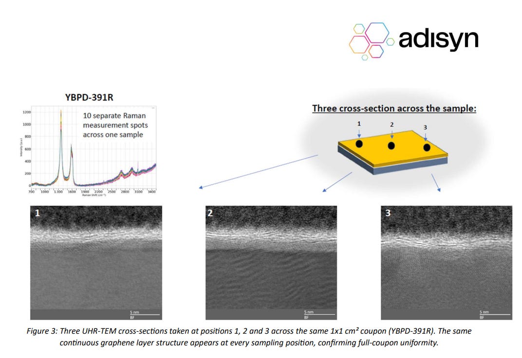
A patchy layer is no use inside a chip. So they sampled the graphene at three different points across the surface, and it was the same at all of them.
Repeatable run to run, and the same right across the sample. A university lab can manage a one-off. A fab’s production line needs both, every single time.
The result proved a third thing (and this is the one chipmakers get excited about).
Adisyn's process works across a wide band of temperatures, which the industry calls a process window.
Say a process only forms its coating at one set temperature, 350°C and nothing else. Every other step on the production line then has to be built around that single number, which makes it a headache to fit in anywhere.
Adisyn's process runs from below 450°C all the way down under 300°C. The low end keeps it safe on the delicate structures a hotter process would wreck, and the width gives a fab the room to use it at several points along the line and set the temperature where the rest of the process needs it.
A window that wide also opens it up to jobs beyond the interconnect wiring. The more places a fab can slot it in, the more the industry wants it.
The machine Adisyn used, called an ALD system, is the standard tool already sitting in every leading-edge fab on earth. So if TSMC already owns the machine, what are they paying Adisyn for?
Think of the machine as just the oven. Adisyn’s invention is the recipe, the chemistry and the precise process that makes graphene actually form at low temperature inside that oven.
Owning a pizza oven doesn’t mean you can make the pizza. Adisyn owns the recipe to one of the most promising breakthroughs in microchips in a decade, and it’s patented.
That’s the part a fab can’t get anywhere else, and will pay a whole lot for.
Where AI1 Sits Today
A quick catch-up for anyone new to the story.
We got on the register in early April. Inside a week it ran to 20c, topped the ASX gainers board and added around $130 million in market value.
It hasn’t slowed down since.
The graphene process AI1 has cracked points at two very different markets.
The first is the one we’ve been walking through. Inside a chip, graphene grows as the wiring that carries the signal, the job copper can no longer do as chips keep shrinking.
The second is stealth. A radar finds an aircraft by firing out a signal and waiting for the echo to bounce back. Coat that aircraft in Adisyn’s graphene and the echo gets swallowed instead of returned, so a full-sized drone reads on the screen as something closer to a bird.
The same material that fixes the chip also helps a drone fly in unseen.
The news flow since April has been relentless. Adisyn locked in an exclusive worldwide licence on the stealth tech out of Tel Aviv University, then raised $14 million with Israel’s biggest investment house and Regal cornerstoning the book. Then the former commander of Israel’s Iron Dome came on to advise the drone arm, and the US granted the patent that sits over the whole thing.
This week, the chip side took the next big step forward.
What This Unlocks
Until now, Adisyn has been a lab story. A good one, but a lab story. With the result independently verified, the company can stop talking about what the process might do and start showing it to the people who’d buy it.
That means the Tier 1 chipmakers, the TSMCs and Samsungs of the world, and conversations about running the process inside their own fabs.
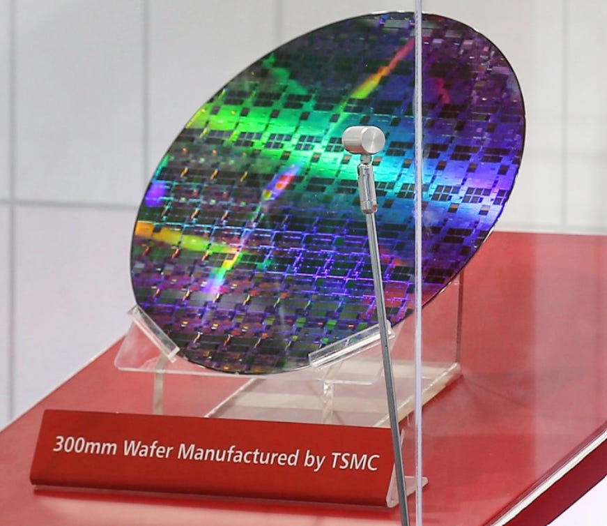
There’s a scaling job to do first. Everything so far has been grown on a square of copper a centimetre across. A real chip is built on a wafer, a silicon disc up to 300 millimetres wide, and Adisyn has to take the process up to that size before a fab can run it for real.
Think of it as proving the recipe works in the test kitchen, then proving it works in a restaurant turning out a thousand plates a night.
Then comes the part every small-cap is ultimately judged on. The science can be brilliant, but a company only gets rewarded once that science starts earning.
Adisyn’s path to that is licensing.
It owns the patented recipe, the fabs own the factories, and the cleanest model is to let them run the process and collect a royalty on every wafer that comes off the line.
A process this central is also an asset a major could simply decide to buy outright.
When the industry last switched interconnect material, from aluminium to copper, the chipmakers went out and bought the new chemistry from specialists.
Graphene is also one of the best heat conductors known. AI chips are built by stacking smaller chips tightly together, and packed in like that they run hot. Cooling those stacks could be where the graphene side brings in its first revenue.
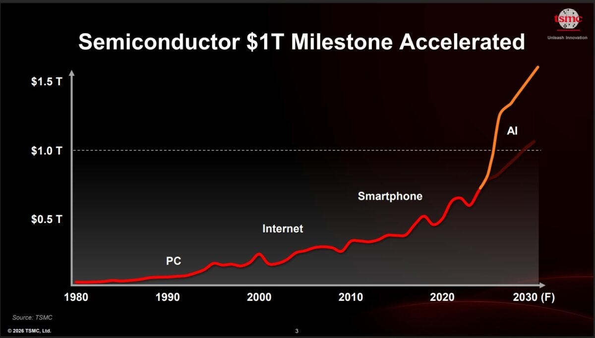
The global semiconductor market is tracking towards US$1 trillion next year, and Adisyn’s process plugs straight into the interconnect segment, the wiring sitting inside every advanced chip. That segment is worth around US$31 billion today and headed for US$45 billion by 2035.
Now weigh it against the company carrying it. Adisyn’s whole market value wouldn’t cover the fit-out of one corner of a multi-billion dollar TSMC fab, and it owns the patented recipe the giants are going to need.
What We’re Watching From Here
The next domino is a million-dollar cheque.
Adisyn’s stated target is a binding deal with one of the global chipmakers, worth north of a million dollars to AI1, and the first of what could be many. For a company this size, that first name on a contract would land like a bomb.
Then watch who comes to the table. Adisyn is about to walk into TSMC, Samsung and the rest carrying results nobody can hand-wave away and a US patent in its back pocket, and the names that lean in, plus how fast they do it, will tell the story louder than any ASX release.
The giants will take their time. They test a new process half to death before they let it anywhere near a production line, so the conversations Adisyn is about to start will run on their clock. Worth remembering for anyone expecting sales by tomorrow.
While they get comfortable, we’re sitting on the one company that’s already cracked the thing every last one of them needs.

Our View
Step back from the nanometres and the interconnects for a second.
The most advanced industry on earth has been stuck on the same problem for a decade, and this week a small-cap on the ASX put a verified answer on the table.
Signed off, no less, by a man who learned graphene standing next to the bloke who won the Nobel for it.
Something this big usually sits locked inside a university lab, or buried in a research budget at TSMC. This one trades on the ASX.
The hard science is progressing quickly, and what’s coming is the selling, to buyers who are already telling the world that graphene is the future.
Every target the company has set itself, it’s gone and hit, and now it’s handed the proof to someone with no reason to flatter it.
A Nobel Prize was handed out for discovering graphene.
The fortune goes to whoever works out how to deploy it at commercial scale.