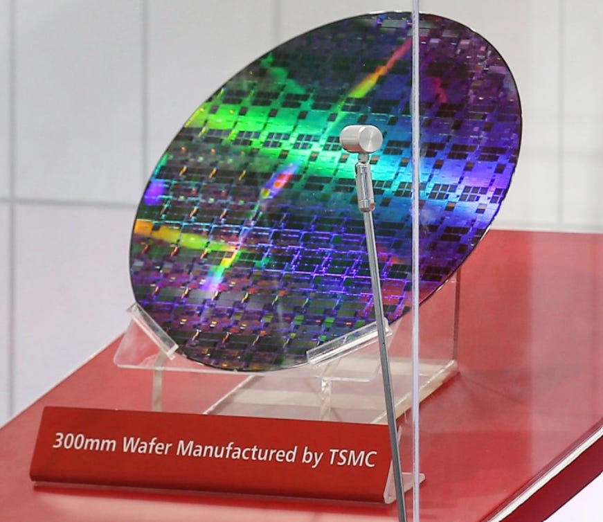
In June we told you Adisyn had cracked the recipe the whole chip industry had been chasing. They grew graphene below 300°C, comfortably under the heat ceiling that had beaten everyone else, on a square of copper about a centimetre across.
We also told you what had to happen next, the process had to scale from that little square up to a full-sized industrial wafer.
In culinary terms, the test kitchen had proved the dish but needed it to work in a restaurant turning out a thousand plates a night.
Less than two months later, Adisyn (ASX: AI1) has walked out of that kitchen carrying a dinner plate. A full 200mm industrial wafer, the format behind hundreds of chip production lines worldwide, covered edge to edge in graphene.
The wafer was tested at 12 points spread right across the surface, and every one of them came back with graphene confirmed, verified independently at the Hebrew University of Jerusalem.
Nobody has ever publicly shown graphene grown this cold across a full industrial wafer before. Anywhere.
And the door it opens leads into hundreds of chip production lines around the world…
What Adisyn Actually Did
The wafer is a disc 200 millimetres across, about the size of that dinner plate, and the format is what's fed into production lines from Texas to Taiwan every day. Adisyn's was copper, the same metal its graphene grows on.
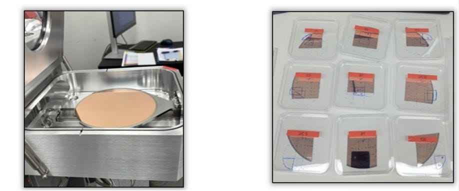
Adisyn grew its graphene across the most valuable wafer in the company’s history, below 300°C again, and covered 300 times the area it managed in June.
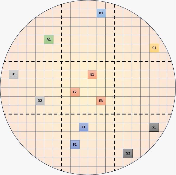
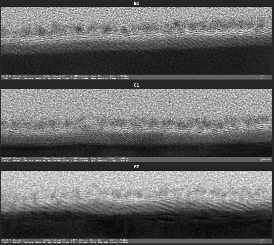
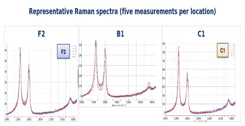
A fab (the industry’s word for a chip factory) won’t take your word for the bits you didn’t test, and a coating a few atoms thick can be flawless in one corner and missing in the next. So 12 points were marked out across all four quadrants, each was measured five times, and samples from all 12 went to the Hebrew University of Jerusalem for independent analysis.
Two machines did the checking. Raman spectroscopy bounces a laser off the surface and reads the light that scatters back, which tells you it's proper graphene at every point tested. Transmission Electron Microscopy is a camera so powerful it can photograph the atoms.
One of the tests confirms the material, and the other shows you the layer sitting in the image. All 12 points passed both.
"Scaling a new materials technology from laboratory samples to a full 200mm semiconductor wafer presents significant technical challenges. Achieving that step - and identifying graphene at all 12 locations independently tested across the wafer - provides important validation of our technology and development approach.”
- Managing director Arye Kohavi.
Why the 200mm Wafer Result is the Front Door
The newest AI chips are built on larger 300mm wafers, so a fair first question is why the older format has us this excited.
Your car helps answer it. There are more than a thousand chips in many new cars, and most of them came off a 200mm line. The chip that flips your iPhone screen sideways when you turn it came off one too.
The supposedly legacy format is also growing. SEMI, the industry's own data house, has global 200mm capacity at record levels above 7.7 million wafers a month, with 13 new production lines coming online through 2028 and capacity heading past 8.2 million a month by 2030.
Call it roughly 92 million wafers a year, with every one of them the format Adisyn has now proven its process on.
It plugs Adisyn directly into the interconnect market and the wiring inside every advanced chip, which is worth around US$31 billion today and growing.
The fabs running those lines are also the likeliest first customers. A specialty fab wins work by making chips its rivals can't, and Adisyn's graphene hands them a new offering to sell.
And what they'd be selling is better wiring. Almost every advanced chip made today runs on copper wiring, and as chips keep shrinking, that copper is hitting its limit. The wires are now so fine they run hot, and power that should be doing useful work leaks away as heat.
Graphene promises to carry the signal with far less of the heat problem, which is why the industry wants it inside the next generation of chips.
What the Wafer Milestone Unlocks
Kohavi says hitting the milestone early shortens the timelines for industry collaborations and integrations. Which is a formal way of saying the chipmaker conversations just sped up.
Until now, every conversation with a chipmaker was likely stalling at the question of “Can this survive a full wafer?”
Now Adisyn can slide the wafer across the table.
300mm is where TSMC and Samsung operate. From here Adisyn chases the 300mm result while the 200mm conversations with chipmakers progress, and the company’s target remains a binding commercial deal with a global chipmaker.
Where Adisyn Sits Today
A quick catch-up for anyone new here.
We first wrote Adisyn up in April at 6.8c. Inside a week it ran to 20c, topped the ASX gainers board and added around $130 million in market value.
Adisyn is attacking two huge markets with the same material. Inside a chip the graphene grows as the wiring that carries the signal. On the outside of a drone it becomes a coating that swallows radar instead of bouncing it back, so a full-sized aircraft reads on a screen as something closer to a bird.
Since April the company has locked in an exclusive worldwide licence on the stealth tech out of Tel Aviv University, raised $14 million with Israel's biggest investment house and Regal cornerstoning, brought on the former commander of Israel's Iron Dome to advise the drone arm, and banked a US patent over the core process.
Then in June came the breakthrough, graphene grown below 300°C and verified by one of the world’s leading graphene researchers at UNSW.
Today that same graphene covers a full industrial wafer.
Who Notices a Result Like This
We filmed this with chairman Kevin Crofton three months ago, back when the graphene covered a single centimetre coupon. His read on how the TSMCs and Intels react when a result like this lands has aged well.
Our View on Adisyn (ASX: AI1)
TSMC, the biggest chipmaker on earth, has already named graphene as the way past copper. Adisyn owns the patented recipe for growing it at a temperature chips can survive, and now it's the first company in the world to publicly show it done across a full industrial wafer.
Adisyn is still pre-revenue, and the giant chipmakers test a new process half to death before it goes anywhere near a production line.
Whatever comes next runs on the chipmakers’ timetable, which is slow, and the 300mm result still has to be delivered.
But the patented recipe belongs to Adisyn, and the giants are the ones who need it. The company's entire market value is still roughly the cost of fitting out one corner of a TSMC fab.
Management told us they’d grow graphene cold, then went and did it. They told us they’d scale it, and this week the wafer turned up.
The next promise on the list is a chipmaker’s signature, and betting against this company keeping their word has been a losing trade all year.
The dinner plate is out of the kitchen. Now we find out who’s hungry.